 N環球

TSMC to Make 3nm Chips at Second Japan Fab, Investment Over $23 Billion
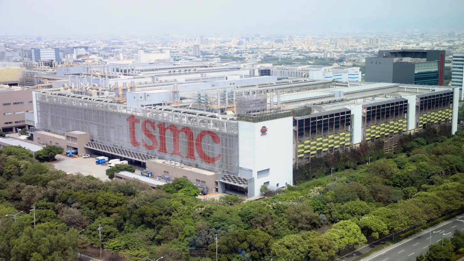
Japan's METI approved a revised production plan for TSMC's JASM second Kumamoto fab: 3-nanometre chips at 6,000 wafers a month, with first shipments in Q4 2028.
Why it matters
This is the first time TSMC's most advanced process node will be made outside Taiwan. Japan's Ministry of Economy, Trade and Industry (METI) approved the revised production plan for JASM's second Kumamoto fab on October 16: the original 6nm/12nm plan from 2024 is replaced with 3-nanometre logic chips at 6,000 300mm wafers a month, with mass production from December 2028, first shipments in the fourth quarter of 2028, and a committed production period of at least 10 years, primarily serving Japanese customers. TSMC's Japan X account confirmed on October 20 that production and investment plans will be implemented in phases based on market demand, with government support as a condition.
Full report
Total equipment investment is expected to exceed USD 23 billion. The Japanese government approved up to ¥645.15 billion (about $4.1 billion) in subsidies for the second fab, below the original plan. TSMC said the facility would meet growing demand for advanced chips driven by AI while supplying technology to customers in Japan and beyond. JASM is a joint venture (TSMC ~86.5%, Sony Semiconductor Solutions ~6%, Denso 5.5%, Toyota 2%). METI also approved a revised plan for the first fab, focusing on 22/28nm and dropping the 12/16nm items. Analysts note 3nm capacity is capped by EUV tool availability, with 6,000 wafers a month being the first phase.
Separately, TSMC and Sony Semiconductor Solutions agreed in August to set up Advanced Vision Semiconductor Manufacturing Corp. in Kumamoto to develop and manufacture next-generation image sensors, with production from 2029.
💬 Comments
No comments yet. Be the first!