 N環球

Samsung chairman Lee Jae-yong visits Yokohama advanced packaging lab, stresses AI chip packaging as competitiveness core
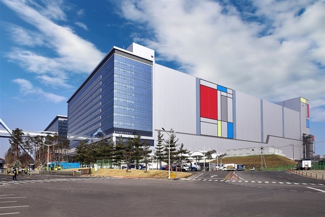
Samsung Electronics says chairman Lee Jae-yong visited its Advanced Package Lab (APL) in Yokohama, Japan, on November 1, reviewing advanced packaging materials and process progress with local researchers and discussing closer cooperation with Japanese materials, parts and equipment firms; it was his first on-site inspection since the lab officially opened on September 8. (Cover photo is a Samsung-related file photo.)
Samsung Electronics says chairman Lee Jae-yong visited its Advanced Package Lab (APL) in Yokohama, Japan, on Sunday, November 1, reviewing the development of advanced packaging materials and process technologies with local researchers and discussing ways to strengthen cooperation with Japan's materials, parts and equipment industry. He urged the team to secure advanced packaging technology, which he described as now central to semiconductor competitiveness in the AI era.
The lab's role: linking Samsung design and manufacturing with Japan's materials ecosystem
According to Samsung, the APL was established in Yokohama in 2023 and officially opened on September 8, 2026; this was Lee's first on-site inspection since the opening. The lab develops and verifies the key materials and process technologies needed for advanced semiconductor packaging, and is positioned as a hub linking Samsung's chip design and manufacturing capabilities with Japan's materials, components and equipment technology ecosystem. Samsung plans to invest about 40 billion yen (about 350 billion won, about $262 million) in the R&D facility over five years starting in 2024. Samsung's announcement mentioned no specific agreement reached during the visit.
💬 Comments
No comments yet. Be the first!