 N環球

Hanmi Semiconductor opens US subsidiary in San Jose to target AI chip packaging market
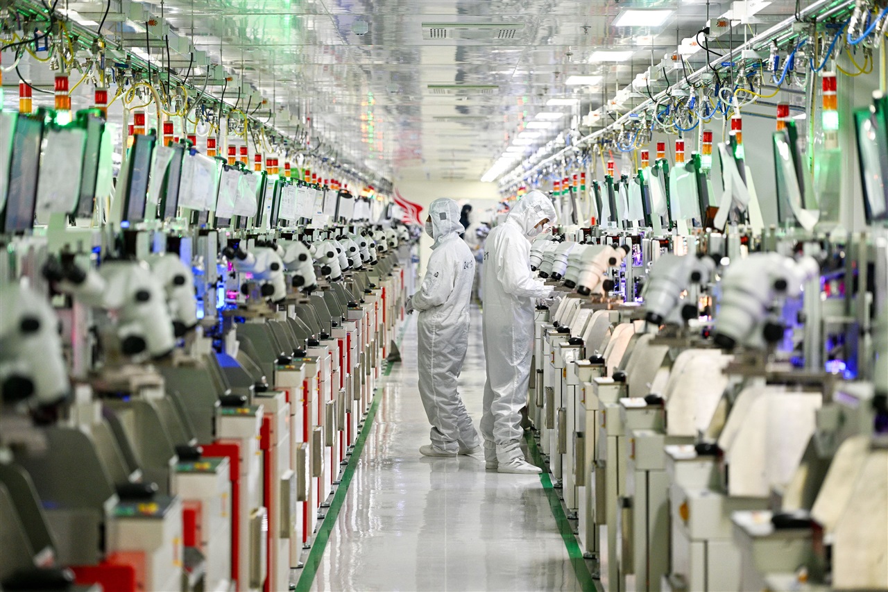
South Korean HBM equipment maker Hanmi Semiconductor announced on October 19 that it has opened a US subsidiary, "HANMI USA," in San Jose, California — its fourth overseas base after Taiwan, China and Singapore — to support the expansion of advanced packaging capacity in the United States.
Why it matters
According to Yonhap Infomax on October 19, Hanmi Semiconductor (KRX: 042700) announced the establishment of its US subsidiary "HANMI USA" in San Jose, California, holding an opening ceremony on October 16. It is the company's fourth overseas base, after Hanmi Taiwan, Hanmi China and Hanmi Singapore, marking the South Korean semiconductor equipment maker's formal push into the North American market.
Full report
Based in Silicon Valley, HANMI USA will provide local engineering support for equipment installation, operation, maintenance and performance optimization, stationing experienced engineers in advance to align with the commissioning schedules of new US semiconductor fabs and advanced packaging plants.
Hanmi's core products are thermal compression (TC) bonders for high-bandwidth memory (HBM) manufacturing and 2.5D packaging equipment, making it a key equipment supplier in the global HBM supply chain. Under the US CHIPS Act, SK Hynix is building an HBM packaging plant in Indiana, while Micron, Intel and Amkor are expanding US investments; Hanmi said it aims to expand supply opportunities for its TC bonders and advanced packaging equipment on the back of this buildout.
Source
Yonhap Infomax, Aju Press, semiconductor-digest, Oct. 19, 2026.
💬 Comments
No comments yet. Be the first!