 N環球

Apple A20 Pro teardown: 2nm silicon in nearly the same area, one more GPU core and a near-doubled Neural Engine
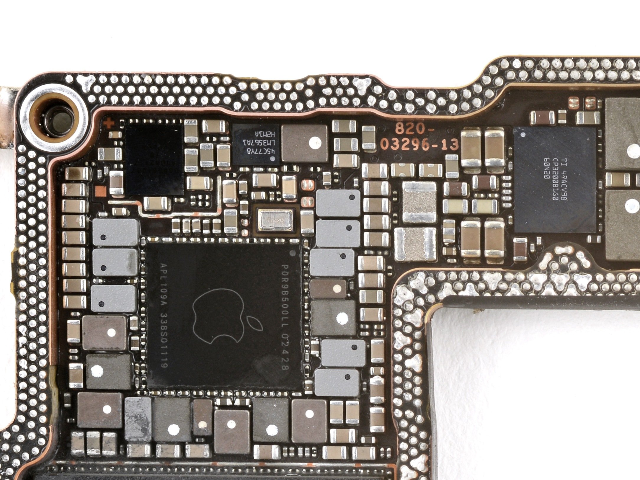
A teardown by TechanaLye, published by EE Times Japan on October 30, shows Apple's A20 Pro in the iPhone 18 Pro moves to TSMC's 2nm process while growing only about 0.6% in die area over the 3nm A19 Pro, yet adds a GPU core and roughly doubles the Neural Engine; the package also switches from stacked to side-by-side memory, with 14 pieces of silicon in total.
WASHINGTON — A teardown of Apple's A20 Pro, the processor inside the iPhone 18 Pro, is out. According to an analysis by semiconductor teardown firm TechanaLye published by EE Times Japan on October 30, the A20 Pro moves to TSMC's 2-nanometer process, from 3nm on the previous-generation A19 Pro; setting the A19 Pro's die area at 1.000, the A20 Pro measures 1.006, an increase of only about 0.6%.
Nearly the same area, stronger compute blocks
The near-flat area hides clear upgrades inside. The teardown shows the A20 Pro gains one GPU core and roughly doubles the size of its Neural Engine (NPU), strengthening on-device compute. That matches Apple's September announcement, which lists the A20 Pro as a 6-core CPU, 7-core GPU and dual 16-core Neural Engine, with 50% more memory bandwidth than the A19 Pro.
New package: memory sits beside the chip, out of the thermal path
The packaging is the other big change. Where the A19 Pro stacked the chip and memory vertically, the A20 Pro places them side by side, moving memory out of the chip's thermal path so the chip can attach directly to a redesigned vapor chamber. The teardown confirms 14 pieces of silicon in the package: one 2nm system-on-chip, six LPDDR5X memory dies and seven silicon capacitors, with 12GB of total memory; the capacitors together cover about 9% of the chip's area.
2nm independently confirmed by a second teardown firm
The 2nm process itself carries a second verification: teardown firm TechInsights published a preliminary analysis on September 22 confirming the A20 Pro uses gate-all-around nanosheet transistors, replacing the FinFET structure that defined leading-edge manufacturing for more than a decade. Two independent teardowns now agree that TSMC's 2nm node is shipping in a mass-market consumer product.
The teardown speaks to hardware structure and scale, not everyday performance, which also depends on software tuning and cooling; Apple attributes its sustained-performance gains to the package, materials and vapor-chamber changes together, without isolating each contribution.
💬 Comments
No comments yet. Be the first!